Photodiode substrate: It is a rigid or flexible substrate that uses thin-film transistor manufacturing processes to produce regularly arranged sensing pixels and circuits on the surface. The main function is to sense, absorb visible light and convert it into electric charge to be stored in the transistor.
a-Si TFT Design & Manufacture
IGZO TFT Design & Manufacture
LTPS Design & Manufacture
a-Si Photodiode Design & Manufacture
Flexible & Glass Substrate Manufacture
a-Si sensor array : Two-dimension matrix structure. Each pixel includes one switching thin film transistor (TFT) and one light-sensitive photodiode .
IGZO thin film transistor : IGZO-TFT shows faster read-out speed and lower noise compared to amorphous silicon TFT.
LTPS thin film transistor : LTPS-TFT shows highest mobility compared to amorphous silicon TFT and IGZO TFT.
Flexible Substrate : Has light-weight and non-breakable merits.
Scintillator
Scintillator : Absorb X-ray radiation and convert to visible light.
CsI Direct Deposition Technology
CsI Film Lamination Technology
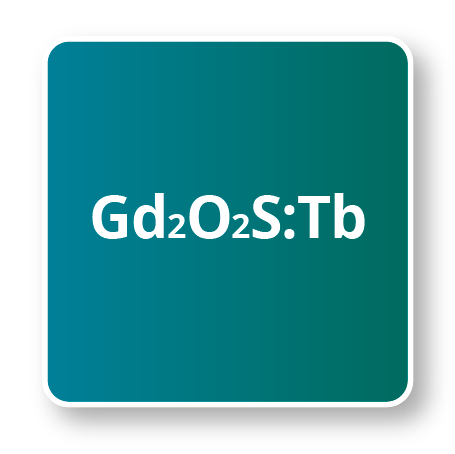
Gd2O2S Film Lamination Technology
Structured scintillators consist of phosphor material in a needle like structure. This increases the number of X-ray photon interactions and reduces the lateral scattering of light photons.
Unstructured scintillators scatter a large amount of light and this reduces spatial resolution. But Gd2O2S:Tb shows low lag image compared to CsI:TLI.